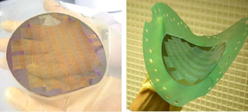
We achieve single event radiation hard microelectronics by thinning full wafers to less than 10 microns (membrane dimensions) and re mounting on carriers.  The wafers shown are mounted on polymer clear transparent polymer carriers. These processed wafers were thinned to less than 10 microns. Chip performance can also be enhanced by straining whilst in membrane format. This increases both output and speed by 20% to 30% in n- and p-MOSFETs. Our patented technique applies mechanical stress to commercially available ICs after their IC processing is complete.
Permanent substrates of different physical properties can be bonded to the membrane wafer.
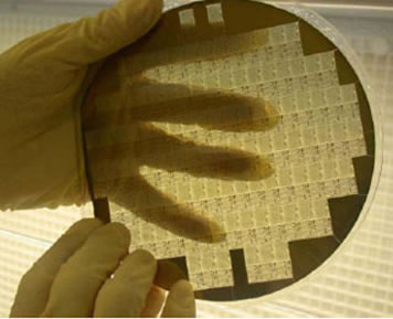
 Here a quartz wafer is the final substrate. Rendering the entire wafer transparent. Strain is kept within the elastic range and so defects are not an issue. We can bond to most any semiconductor permanent substrate. Here is a SOI, Rad Hard strained wafer on quartz, fabricated by the above method in just one of the many permutations possible. Our technique has been successfully applied to bulk, partially depleted and fully depleted architectures.
Belford Research offers an entirely new way to single event radiation hard electronics. Our new post-processing wafer scale technique has attained unparalleled increases in both output and speed. We have Diverged from standard IC processing we have delved into membrane physics. Our techniques are inherently versatile and intelligent. It benefits from a matrix of directional-strain data which the technique itself enables.