Stressing the Benefits of Intelligent Strain
Which straining technique can continue to rescue the shortfalls of scaling: Wafer scale straining or process-induced straining? These current methods have limited use; wafer scale techniques are limited to biaxial strain and process-induced methods are difficult below the 65 nm node. Belford Research offers an entirely new way to strain silicon – mechanically. Our new post-processing wafer scale technique has attained unparalleled increases in both output and speed. Diverging from standard IC processing we have delved into membrane physics. Our straining technique is inherently versatile and intelligent. It benefits from a matrix of directional-strain data which the technique itself enables.
Straining at the Bit
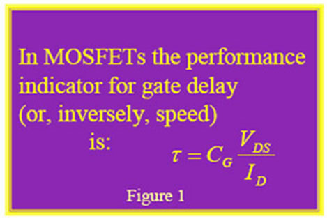 The expected economies of scaling have been eroded in terms of both yield and reliability. Traditionally, one scaling step reduces the channel by 1/3. As the channel length decreases, capacitance decreases and in reality the delay is reduced by 1/2 aided to some extent by velocity overshoot. Scaling from 130 nm to smaller gate sizes has not produced the expected device speed as the gate oxide is ineffective when less than its 130 nm node value (~1.5 nm). Figure 1 shows the dependence of device speed on gate capacitance CG.
Reducing the gate oxide thickness will require new dielectric materials. In the interim, process-induced strain has been cleverly devised to boost speed which is the main driving force for scaling. The industry now relies on strain-enhanced mobility to pick up the shortfall in device speed which in deep submicron systems is governed by the gate oxide thickness (vertically-challenged scaling).
There is little doubt that straining silicon is a viable route to enhanced device performance. Process induced strain is the preferred method for 90 and 65 nm CMOS. It is by far the most attractive in terms of carrier specific needs; n-channels are given longitudinal tensile strain - their favorite - while p-channels get their most effective compressive treatment. However, process-induced strain is meeting its own wall at below the 65 nm node. Industry’s success story has gone from “No Strain No Gain” to “No Strain without Pain”. The reasons for this cut-off are process-limiting aspects; not least being that regional tensile and compressive strain areas may self-cancel when spatially compromised. At deep submicron dimensions the close proximity of tensile (n-channel) and compressive (p-channel) regions can result in strain relaxation. This occurs most readily when the ICs are electrically stressed and local temperatures rise. Re-optimization for each new node is therefore increasingly difficult. This is true for dual-stressed liners, tensile cap layers, and source-drain injections. The latter also suffers from Ge diffusion in deep sub micron regions. As dimensions reduce, device level strain becomes unpredictable as the non-linearity of the strain field is accentuated.
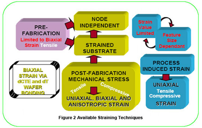
Ideally, wafer scale straining is preferred, but until now this method - whether SOI or Bulk - delivers only biaxial strained, expensive, non-standard, substrates.
We think we have a better process; it has inherent variability and has supplied us with the physical results needed to make informed decisions on strain directionality and defect control. Figure 2 gives a snapshot of the available strain methods and their range of strain delivery. Belford Research’s main technology is amber colored. We also have a different emerging technology involving dCTE wafer bonding to create SSOI. We patented this concept in 1999 but only recently gained the funds to realize it. Initial work has been successful but it is still in the research stage (skeleton block in the diagram).
The entire range of strain effects is not at all obvious. The knowledge base is confined to available straining methods and is segmented in separate small pieces like a jigsaw puzzle. Intelligent use of strain would be so much easier if we could solve the puzzle and match up the pieces to see the entire picture. Straining optimally requires understanding fully the consequences of directional strain, engineering its benefits, and avoiding its pitfalls. Optimum strain for ultimate CMOS performance has not been achieved and this optimum can vary depending on channel size and layout. Belford Research has been able to answer some of the fundamental questions and has completed the framework for the puzzle by straining processed-IC-membranes mechanically. We have gathered a matrix of information from a range of device types and sizes, varying strain direction and using, to different extents, combinations of longitudinal and transverse in-plane stresses.
Defining Strain
We believe the key to understanding strain is to understand just what its variables are, and how they affect conduction. The variable parameters can be listed as follows; firstly there is compressive or tensile strain. Each of these can be applied biaxially or uniaxially (totaling four variables) and uniaxial strain has a further two variables, as it can be applied in two different directions, transverse or longitudinal to the carrier flow. Each of these six different types of strain alter electron and hole mobility differently (totaling twelve variables). The list presents a formidable range for investigation and yet all of these still don’t touch on the critical factors (for future IC production) of channel length dependence and optimum strain level.
Diagnostic Strategy
Prior to launching into our technology which provides strained wafers in standard format, we gathered diagnostic information by interrogating devices during the straining process. We custom built a mechanical stressor in-situ within our probe station. Processed wafer sections were thinned to less than 10 microns (membrane dimensions) on a polymer carrier.
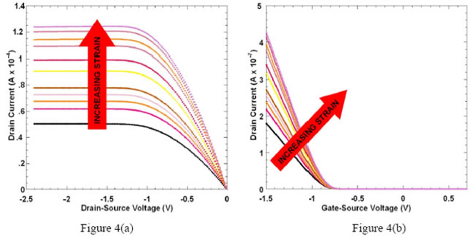
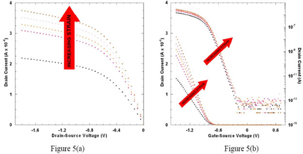
 Mechanical in-situ stress was applied and the devices characterized. This stress/characterization sequence was repeated until the devices failed. Using this method we were able to obtain the following types of strain; uniaxial tensile strain in any direction; biaxial tensile strain and anisotropic biaxial strain; it was also possible to induce compression. An example of the strain diversity possible and the information available is shown in Figures 3 through 6. Devices tested were partially depleted large (square) and short channel pMOSFETs of the same width. Figure 3 shows the stresses applied which gave the results shown in Figures 4 and 5.
Figure 3
Figures 4 (a) and (b) give the output and subthreshold of a large square channel pMOSFET and Figures 5 (a) and (b) give the output and subthreshold of a short channel pMOSFET. The biasing conditions are identical. The different traces correspond to different amounts of strain. The only difference between Figures 4 and 5 is that the device channel in Figure 5 is shorter. This experiment gave information on strain combination type and channel length dependency. The output increase in the longer channel is 250% while the output increase in the shorter channel is only 75%. These devices were characterized before strain, strained sequentially within the probe station and interrogated at each strain level under identical biasing conditions. Using this sequence of stressing and device characterization, many strain variations have been investigated and a matrix of information has been compiled.
Mechanical in-situ stress was applied and the devices characterized. This stress/characterization sequence was repeated until the devices failed. Using this method we were able to obtain the following types of strain; uniaxial tensile strain in any direction; biaxial tensile strain and anisotropic biaxial strain; it was also possible to induce compression. An example of the strain diversity possible and the information available is shown in Figures 3 through 6. Devices tested were partially depleted large (square) and short channel pMOSFETs of the same width. Figure 3 shows the stresses applied which gave the results shown in Figures 4 and 5.
Figure 3
Figures 4 (a) and (b) give the output and subthreshold of a large square channel pMOSFET and Figures 5 (a) and (b) give the output and subthreshold of a short channel pMOSFET. The biasing conditions are identical. The different traces correspond to different amounts of strain. The only difference between Figures 4 and 5 is that the device channel in Figure 5 is shorter. This experiment gave information on strain combination type and channel length dependency. The output increase in the longer channel is 250% while the output increase in the shorter channel is only 75%. These devices were characterized before strain, strained sequentially within the probe station and interrogated at each strain level under identical biasing conditions. Using this sequence of stressing and device characterization, many strain variations have been investigated and a matrix of information has been compiled.
Results are easily repeated and we have actually increased mobility and output simultaneously beyond 300% for individual p-MOSFETs using this combination of strain. However this particular combination of strain is detrimental to n-MOSFETs and as the driving force of the investigation is CMOS enhancement this strain combination is not viable. Electrical stressing and elevated temperature cycling gave the same results as the pre-strained wafers.
BRI’s Straining Technique
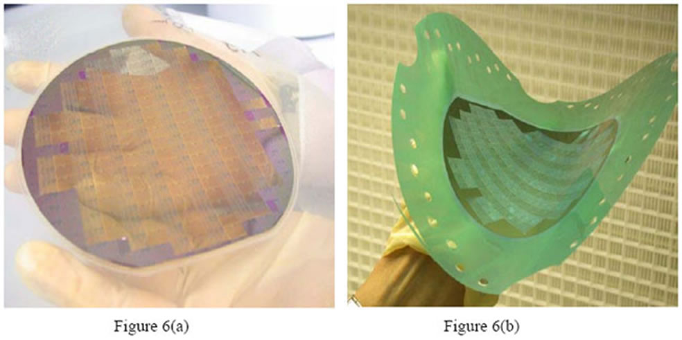
We have reproducibly achieved simultaneous increases in both output and speed by 20% to 30% in n- and p-MOSFETs. Our technique is to apply mechanical stress to commercially available ICs after their IC processing is complete. Wafers are thinned to less than 10 microns (membrane dimensions) and are mounted on a polymer carrier. Figure 6 (a) shows a thinned wafer on a clear transparent polymer carrier. Figure 6 (b) shows how flexible these membranes are. Tensile stress is applied in one or more directions and a permanent substrate is bonded to the wafer while it is held under tension.
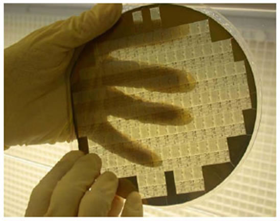 The resulting planar format is essentially the same as the starting wafer. Strain is kept well within the elastic range and so defects are not an issue. We can bond most any semiconductor material as the permanent substrate and so create SOI and Radiation Hardened ICs from bulk architectures. Figure 7 shows a biaxial strained wafer on a quartz substrate, fabricated by the above method in just one of the many permutations possible. Our technique has been successfully applied to bulk, partially depleted and fully depleted architectures. Work is underway in producing a fab-friendly process which would slot in-between wafer thinning and packaging.
Belford Research, Inc. was formed to create physical/mechanical techniques to strain semiconductors, and, to exploit the strain-induced change in electronic and optical properties. We have accomplished the technical goals.
The resulting planar format is essentially the same as the starting wafer. Strain is kept well within the elastic range and so defects are not an issue. We can bond most any semiconductor material as the permanent substrate and so create SOI and Radiation Hardened ICs from bulk architectures. Figure 7 shows a biaxial strained wafer on a quartz substrate, fabricated by the above method in just one of the many permutations possible. Our technique has been successfully applied to bulk, partially depleted and fully depleted architectures. Work is underway in producing a fab-friendly process which would slot in-between wafer thinning and packaging.
Belford Research, Inc. was formed to create physical/mechanical techniques to strain semiconductors, and, to exploit the strain-induced change in electronic and optical properties. We have accomplished the technical goals.